Electronic Design

Connect Tech's Qseven at core of military VR system

Connect Tech, based in Ontario, Canada, designs and manufactures serial communication hardware and software for a range of industries, including communications, industrial automation, transportation, government, military, scientific, medical, educational, POS, and office automation. At DesignWest, they exhibited a military training system from Quantum3D, that was driven by custom single-board computer, built on Connect Tech's Qseven Carrier board with an Intel® Atom™ processor.  New Tech Press dropped by and had a bit of fun with the team.

Learn more at element14.com

Tying the home to the Smart Grid

Most of the attention in the Smart Grid is given to the utilities and their controversial wireless smart meters.  But for the consumer to see real value in the technology requires creating a local network of appliances and systems within the home. That's not an easy task. There are many smart appliances on the market ready to tie into the grid, but not everyone is flush enough to go out an buy an entirely new set of appliances.  Somehow, the industry needs to create aftermarket.  At the DesignWest conference, Qualcomm Atheros was demonstrating your their products and techniques can move you closer to  energy efficiency, if not complete independence.  New Tech Press interviewed Qualcomm Atheros product manager Tim Colleran on what's happening.

Nabto offers development help for their worldwide firewall

Security in the "Internet of Things" is becoming a major issue in embedded, portable device industry and the tiny Danish company of Nabto is helping customers take a step toward securing new devices.  At DesignWest, Nabto was talking about the Nabduino, a Arduino-based development board with their tiny (less than one meg) webserver IP that can place your device behind the corporate firewall...anywhere in the world.  New Tech Press dropped by to chat with them.

Screaming Circuits finds silver lining in economic downturn

The economic downturn has had an upside for some industry segments. PCB prototyping service Screaming Circuits has seen business climb steadily since it's founding in 2003 as more companies have cut back staff and resources, stretching engineering staffs beyond their own capabilities. Screaming Circuits recently formed a relationship with Newark/element14 to offer their services to the element14 community. In this interview with Duane Benson, director of marketing and sales, Benson elaborates on the growing prototyping market in the PCB industry as well as the challenges and needs of their customer base.

Rising custom IC costs could eat into Apple's nest egg

By Lou Covey, Editorial Director It's time to stop wondering what Apple is going to do with its cash reserve after it pays out dividends to stock holders.  If what Cadence's Tom Beckley says about the next generation of chips holds true, Apples is going to need every dime to create the next generation of processors for the iPad and iPhone.

Beckley, senior vice president of R&D in the Cadence Custom IC group, was the keynote speaker at the 2012 International Symposium on Quality Electronic Design in Santa Clara (ISQED) addressing "Taming the Challenges in Advance Node Design."  Beckley pointed out that Apple has been the poster child for cost-efficient development and production, but even if every chip developer followed the "Apple Way" it would not put much of a dent in the total cost for developing the next generation of SoCs.

The A5 system on chip in the current Apple products, designed at 45nm, could come in under $1 billion to design and bring to market with effective control of the supply line.  Cost projections for a chip at 28nm (the next step) could be as much as $3 billion. At 20nm, the cost could exceed $12 billion (if you build your own fab, which Apple could well afford.)  The Cadence exec stated that the cost of EDA tools (both purchased and developed) could run as high as $1.2 billion alone.

The evidence of the increasing costs of development can be seen in the profit margins of the iPad.  According to iSuppli, the cost of the A5 chip in the new iPads at $23 is double the cost of the original A4 chip.  Why is the cost going so high?  Because the way chips are being manufactured is changing dramatically.

Beckley explained that the physics of making a semiconductor mask reached a breaking point at the current most popular nodes as the resolution of a photoresist pattern begins to blur around 45nm.  Double patterning was created to address that problem at 32nm.  "But everyone wanted to avoid doing it at 32nm because of the mask costs.  They wanted to maximize their investment in lithography equipment."

The process splits the design where the structures are too close together, into two separate masks.  It's an expensive process (especially when each mask costs around $5 million) and requires entirely new ways of creating the masks to avoid rule violations.  But where the foundries were willing to let is slide at 35nm, they are requiring double patterning at everything below, Beckley stated.

These new techniques are driving up development costs straight up the design chain.  Beckley said he has close to 400 engineers in his unit working on tools just for 20nm design -- half of his entire staff.

The benefits of the moving the node are just as tremendous, he said.  Instead of millions of transistors, each chip will have billions allowing for greater functionality in devices.  "We expect improvements  of 25-30 percent in power consumption and up to 18 percent overall perform and improvement," he predicted.

"If what I'm saying scares you, it should.  There are many questions and issues to be ironed out," Beckley concluded.  "But at Cadence we are already working with a dozen customers on active test chips, which will increase to 20 very soon, and we are already working with customers for products at 10nm."

What are you doing to overcome the rising cost of custom ICs?  Join the discussion at element14.com


Interview with BOM Financial Investments

The Brabant province straddles the border of Belgium and the Netherlands. To the south it reaches into the Belgian capital city of Brussels the home of IMEC, arguably the leading nanotech research center in the world. To the north it comprises most of the Dutch southern communities and the home of the High Tech Campus in Eindhoven. New Tech Press sat down with representatives from the northern province Marcel de Haan, Director of Strategic Acquisition and Bodo DeWit, senior project manager, to talk about the one-stop-shop for technology companies looking to expand into Europe.


UBM survey shows interesting trends in prototyping

UBM released some of the findings of its annual Embedded Study at a special press breakfast on Tuesday at Design West, with some fascinating potential for engineers looking to make the "next big thing" in electronics. The first surprising bit of information is that 26 percent of the respondents reported they were using in-house and Linux-based RTOSes with grow-your-own systems jumping 30 percent.  This is bad news for proprietary commercial providers who have traditionally seen in-house software as its primary competitor.  The primary reason for the jump is the engineers prefer software where they can access the full source code.  That one bit of information should be good news for commercial provider Micrium (element14 supplier) that does offer the source code.

More importantly for developers is the news for Arduino.  The survey asked what chip the are considering using in their next project and 15 percent said Arduino boards.  Holland said the respondents may not have understood the question, since Arduino is not a chip but a board, but a couple of slides later, Holland pointed out that the number of engineers planning on using an FPGA in their next project dropped... by about the same number of engineers.  One could make the correlation that Arduino development boards are replacing FPGAs at least in prototyping.

After the breakfast, Jeff Jussel, senior director for technical marketing at element14, said he could see that correlation when you look at the rising sale of Arduino boards from element14.  "It makes sense," he stated.

Raspberry Pi to narrow Digital Divide?

By Lou CoveyEditorial Director 

The effort to close Digital Divide -- the separation between those who can and can't afford access to the Internet -- has been a point of frustration for government and social activists for more than a decade. However, the rousing success of the Raspberry Pi computer launch on Leap Day could significantly close the Divide with the right price point and distribution strategy and punch a hole in commercial efforts to derail low-cost computing.

The United Nations established the World Information Society Day (May 17) for the first time in 2001 and since then there has been a steady stream of programs and products aimed at closing the divide, from the One Laptop per Child (OLPC) non-profit organization to Intel's Classmate PC.  Even the popularity of netbooks and tablets demonstrated the demand for low cost "ports" to the internet.  None, however, have made a significant dent in the problem.  In the US, where the gap is the smallest, 22 percent of the population still lacks internet connectivity, a figure that has barely improved since 2000 (Internet World Stats).

Several issues continue to dog efforts to close the divide: usability, price and supply. OLPC entered into competitive issues with suppliers early on and is still struggling to bring the devices to below $100 without significant charitable and government subsidy.  Intel, in particular, cut ties with the organization over the price per unit and launched the Classmate PC with greater functionality, and made it difficult to the OLPC offerings to gain significant market presence.

The long-anticipated Raspberry Pi, however, smashed the $100 barrier with a $35, fully internet enabled, credit-card sized device, manufactured and distributed by several sources, including Premier Farnell.  The current version is in one, uncased configuration, powered by an ARM-based Broadcom system on chip, with two USB slots, 256MB of RAM, HDMI slot, SD memory card slot and an Ethernet port, running Fedora Linux OS.

The primary target for the device is education, especially below the college level, but according to Jeff Jussel of element14.com, Premier Farnell's engineering community, the foundation's wants to build an open user community of experienced engineers first, to provide essentially free resources for students to learn how to use the technology. "The Foundation really designed this for education - to give schools and students an exciting platform for rekindling interest in programming.  I think this is the most exciting computing platform for education since I had my first Apple IIe as a kid." (hear full interview with Jussel)

Hence the partnership with electronics distributors rather than chip and system manufacturers. Enter the first problem: While both the foundation and distributors anticipated a significant demand for the product, they had no idea how big it would be.

"We made a limited run," said Jussel, "just to see how fast they would go and we knew we would run out of inventory early on. We thought initially demand would be in the thousands."  That was an understatement.  Worldwide demand exhausted the inventory in two hours and caused the servers for both the distributors and the foundation to crash briefly.

"Demand was actually in the 10s of thousands," said foundation co-founder and executive director Eben Upton (hear interview with Upton).  "We knew we had something special.  We just didn't know how special."

Orders came in primarily from the developer community, as anticipated, leaving very little for education at the outset.  Upton admitted that marketing efforts to education have been focused almost exclusively to the United Kingdom where the government has provided significant support.  In the US, however, not only is Raspberry Pi seen as a misspelled dessert, alternatives like Beagleboard and Cotton Candy are also unknown outside of colleges.  New Tech Press contacted several secondary education technology leaders who did not know of any of the options.

Woodside High School in Redwood City, California has been nationally recognized for its innovative approaches to using and teaching technology, including being competitive in national robotics competitions has yet to use any of the options, and the faculty had not yet heard of Raspberry Pi. David Reilly, principal at WHS said options like Cotton Candy, in excess of $100 would be outside of the budgetary restraints of even the most well-off schools, but the $35 Raspberry Pi might actually been doable.

Jussel said Premier Farnell, through its element14 online community, will soon be launching a program in the US not only to raise awareness of the technology, but to get samples into the hands of educators by the beginning of the start of the new school year.

Once the education market is penetrated, Upton hopes the next step is attacking the Divide.  Upton said the foundation's program began 6 years ago to deal with an ever increasing lack of programming skills of students entering the Cambridge University computer sciences programs.  A study showed that many of the students had no regular access to computers prior to enrolling, a problem that seems to be increasing in families below the poverty level in developed countries.  The availability of a fully functioning, low-cost computing system could rapidly close the gap as long as students had the ability to learn how to use them.

In the US, according to the AC Nielsen company, low-income minority families are more likely to own smart phones and high-definition televisions, than middle income white families, but less likely to own a personal computer.  The families use the phones as their internet connection because the phone and data service are more cost effective than a high-speed cable connection.  Upton said the Raspberry Pi was specifically designed to be able to be plugged into a phone, keyboard and HDTV to keep the overall cost for the system below $100.

How can the engineering community and electronics industry use Raspberry Pi to help achieve the ultimate goal of closing the Digital Divide?  Join the conversation with your ideas at www.element14.com.

The roads less traveled around multicore walls

By Loring Wirbel and Lou CoveyA New Tech Press Report from Footwasher Media

For the better part of two decades, the processor industry has been running pell mell down the road of multicore design, packing more and more processor cores on a single chip.  But a funny thing happened on the way to the personal super computer.  It didn't work.

In 2007, a DARPA study on the potential of an exascale computer concluded that with the current architecture of processors, in other words x86 and PowerPC, we could not get there from here.  As a result, in January 2012, DARPA announced the Power Efficiency Revolution for Embedded Computing Technologies, (PERFECT), to figure out what to do next.

Dr. David Patterson, a RISC pioneer and a leading voice in the development of multicore processors, suggested that the problem could be solved using FPGAs as an experimentation platform in a program he called Research Accelerator for Multiple Processors (RAMP) at UC Berkeley.  In a series of RAMP presentations.  In a related 2006 Berkeley white paper, ‘The Landscape of Parallel Computing Research: The View from Berkeley,’ Patterson said that the power consumption of the logic in the CPU, converted into heat, limits the performance.  Since any heat that cannot be removed by a heat sink reduces the performance of the transistors, the results are:

  • If you increase the system clock to boost performance, heat rises, transistors slow down
  • If you increase memory bus width and you increase the number of transistors, heat will increase and transistors slow down
  • If you increase instruction-level parallelism (ILP) so more can get done at the same time, you increase the heat and...

The result of the RAMP effort?  "The memory wall has gotten a little lower and we seem to be making headway on ILP, but the power wall is getting higher," Patterson said.  One anonymous engineering wag pit it more succinctly,

"We're screwed."
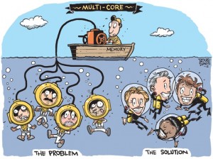
Throughout this process, however, there have been voices, crying by the roadside as it were, "Go back! you're going the wrong way!"  And it may be time for those voices to be heard.

Going back to the turn of the century, companies like the UK-based Celoxica, were pointing out the weaknesses of the multi-core approach in contrast to a heterogeneous approach incorporating FPGAs.

"The first problem is the architecture of the standard processor doesn't lend itself to parallelism," Said Jeff Jussel, former VP of marketing for Celoxica and current senior director of technical marketing for Element14.  “No matter how many processors you put on a chip, we are not seeing any one algorithm processing faster because it is too hard to program access to all the processors.  What you end up with is a system that can do 12 things, but no actual system speed increase with an incredible power increase."

Celoxica's approach, according to Jussel, was to break up the algorithm over multiple processors inside the FPGA with dedicated memory.  "You end up with millions of tiny processors optimized for the algorithm.  When the algorithm changes, you just reprogram the FPGA."

At the time, the problem was not immediate and the market was entrenched. Celoxica ultimately spun off their tool business, eventually landing in the hands of Mentor Graphics and kept their board development business.  That business was always focused on one-off applications, ranging from mining to financial services.

Patterson said their work in RAMP showed that an FPGA approach, especially for highly focused applications, was "more and more attractive" but there were two specific obstacles: power and design tools.  "We found the CAD tools available were just not that easy to work with.  We were actually surprised at how difficult it was and it formed a major stumbling block.  And while FPGA providers have gotten better with power even as the number of transistors increase, they still need to get better with it before it can be a mainstream answer."

The reprogrammable nature of an FPGA has allowed several board- and system-level companies, ranging from Wall Street FPGA in financial analysis markets to Convey Computing in scientific analysis, to assign ARM cores or small hard-configured RISC blocks like MicroBlaze, to a variety of tasks, with subroutines handed off to coprocessors on the same FPGA.  But the dream of a fully retargetable FPGA system, touted in the mid-2000s by companies like Quicksilver, has been largely deferred because of the problem of developing parallel multithread software for such changing architectural types.

Think "many" not "multi"

ARM walks into the fray almost in a position of neutrality.  While it still endorses the validity of Intel's homogeneous approach to multicore, as early as last fall it began discussing a "many core" as opposed to multicore approach.  According to John Goodacre, program manager in the ARM Processor Division, the traditional approach of using full-performance cores still has a long road ahead of it, especially when you are considering dual- and quad-core designs, but it may not be necessary, especially in some consumer applications to use the large cores.

"Mobile applications are full of little processes." Goodacre explained."If you put all those processes into four or eight big cores, you don’t actually see a big performance improvement, but you see quite a big negative power impact. A Many-/multi-processing approach duplicates the capability of a big homogeneous multicore design that is inherently more power efficient."

Goodacre points to ARM's big.LITTLE concept that marries an A15―which he claims is capable of running more of today’s dual-core type software, with four small A7 cores, in a power efficient formation.

"This approach is mostly targeting toward power, but it’s also giving the next generation programmers the concept that there’s also a lot more power efficient processes available for that next generation of software.  The first next generation software I anticipate will be in gaming, but as time progresses and more and more availability of more cores, there will be more software available."

From the software side

Architecture experts developing RISC instruction sets for a mix of server and embedded applications – dominated by ARM, but also including MIPS, Tensilica, and other companies – have offered their cores to standard IT developers, to FPGA and ASIC vendors, and to embedded specialists.  Xilinx and Altera, among other FPGA vendors, say they see a mix of SMP and asynchronous RISC implementations.  Some ARM licensees, including Freescale Semiconductor, Texas Instruments Inc., Qualcomm Inc., and Broadcom Corp., utilize ARM as part of non-SMP designs that use a central control-plane processing environment, in conjunction with on-chip coprocessors for functions such as encryption, deep packet inspection, and fast list searches for tasks such as routing.

See the full story at element14.com and additional coverage at EDN.com.

ISQED Symposium

Title: ISQED Symposium
Location: Techmart Center, Santa Clara, California
Link out: Click here
Description: The International Symposium on Quality Electronic Design (ISQED)—the premier Electronic Design conference—bridges the gap between Electronic/Semiconductor ecosystem members providing electronic design tools, integrated circuit technologies, semiconductor technology,packaging, assembly & test to achieve design quality.
Start Date: 2012-03-19
Start Time: 09:00
End Date: 2012-03-21

The future of multicore and 3D approaches at ISQED

As multicore processor design hits power, memory and ILP walls with increasing frequency, the established methodology is pinning much hope on 3D heterogenous approaches.  Those efforts will be described in detail in a series of best practices tutorials at this year's ISQED symposium March 19, in the Techmart Center in Santa Clara, California. Brian Leibowitz of Rambus Inc. will review the key specifications of memory subsystems and evaluate the advantages and limitations of a variety of design techniques such as low swing signaling, resonant clocking, DVFS, and fast power state transitions, as well as those of emerging 3D packaging methods.

Puneet Gupta, University of California, Los Angeles will address scaling of physical dimensions faster than the optical wavelengths or equipment tolerances used in the manufacturing line leading to increased process variability and low yields which make design process expensive and unpredictable. "Equivalent scaling" improvements - perhaps as much as one full technology generation, can come from looking "up" to circuit design.

As the semiconductor industry migrates toward extreme monolithic foundry level 3D heterogeneous structures for mixed-signal components and systems, Farhang Yazdani, president of BroadPak Corporation, will argue that 3D silicon/glass interposer and through silicon via (TSV) technology will play a significant role in next generation 3D packaging solutions.

Rafael Rios senior researcher in the Manufacturing Group at Intel, will explore the innovations that lead to extending Moore's law into nano-scale feature sizes, including advances in device design, computational lithography, and materials engineering. We will also explore current research work looking into extending Moore’s law into the future.  Hsien-Hsin S. Lee, Georgia Institute of Technology will focus on  die-stacked 3D integration as the frontrunner technology to continue Gordon Moore’s prophecy in the vertical dimension. Stephen Pateras, product marketing director for Mentor Graphics Silicon Test Solutions group, will contend that 3D IC offers a compelling alternative to traditional scaling for achieving advances in performance, reduced power consumption, cost reduction, and increased functionality in a small package.

Article sponsored by Element14.com

Wireless Technology: Where we’ve been and where we’re going

Following is a Footwasher Media interview with Fanny Mlinarsky, President of octoScope, sponsored by element14. We discuss next generation OFDM and MIMO techniques and how they are evolving from the LTE and 802.11n technologies to the emerging technologies being developed for LTE-Advanced and 802.11ac solutions .

FM: Simply put, both technologies are evolving to run faster over a longer range and to support multiple simultaneous transmissions in the same space and frequency channel.

Faster data rates are achieved through the use of wider channels, higher orders of MIMO (multiple input multiple output) and higher order modulation. Although marketers refer to LTE as 4G, officially only LTE-A has been declared 4G by the ITU (International Telecommunications Union).

NTP: Does the new spatial multiplexing feature mean that we are NOT now running out of spectrum space as previously reported?

FM: Due to the scarcity of licensed spectrum, LTE-A has different challenges from those of 802.11ac that has over 400 MHz of spectrum in the unlicensed 5 GHz band. Licensed spectrum typically comes in slivers of a few MHz.  Thus, to increase throughput, LTE-A has introduced spectrum bonding of non-contiguous bands.  To accommodate a higher density of users, LTE-A supports small, short-range base stations, which calls for better management of cell-edge interference through CoMP (Coordinated multi-point) and ICIC (Advanced inter-cell interference coordination) techniques.

A data rate of 6.9 Gbps is achievable, or at least defined in the IEEE 802.11ac draft specification, “IEEE P802.11ac™/D1.4”.  Achieving 6.9 Gbps requires QAM256 modulation and support for 8 spatial streams in a160 MHz wide channel.  LTE-A is expected to reach up to 1 Gbps DL (downlink) and 500 Mbps UL (uplink) rates in a 100 MHz wide channel.

NTP: What new design considerations do these advanced specifications introduce for Wireless System Designers?

FM: MIMO algorithms use multiple synchronized radios (up to 4 for 802.11n and LTE; up to 8 for 802.11ac) to adapt to continuously changing conditions in the wireless channel.  These techniques include:

  • TX and RX diversity to add robustness to the communications when channel conditions are challenging (e.g. low SNR or high multipath)
  • Spatial multiplexing to increase throughput by sending multiple simultaneous streams when channel conditions are favorable
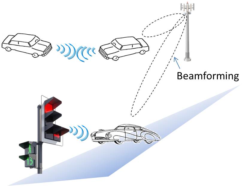
  • Beamforming to extend range and to enable MU-MIMO (multi-user MIMO)
  • MU-MIMO to enable multiple stations to transmit simultaneously in the same frequency channel by focusing the antenna pattern. (See figure 1 above)

MIMO radios sense the conditions in the channel on a packet-by-packet basis and make instantaneous decisions on which of the above techniques to employ.  Testing of these radios requires new generation over-the-air (OTA) technology, such as the octoBox controlled environment OTA test station.

NTP: How do the advanced solutions benefit engineers or humanity at large?

FM: Aside from the obvious fun with video and location-based apps, pervasive connectivity enabled by

Wi-Fi and LTE technologies is poised to help with vital public safety and E-911 communications.  Spectrum in the 700 MHz band has recently been licensed by the FCC to carry a nationwide public safety LTE network, which for the first time will interconnect police, fire, ambulance and other emergency services coast-to-coast for effective management of large scale disasters and incidents.

For engineers, the work is clearly cut out: continue developing connected, location-aware platforms and applications.  Can I poll my refrigerator from the supermarket to download a shopping list?  Can my car sense a red light, while I’m distracted by talking on my smartphone, and apply breaks, avoiding a terrible accident?

NTP: What new features / products / services can end users expect as a result of these new specifications?

The initial release of 802.11ac will operate in 80 MHz channels, enabling over 3 Gbps data rates with throughput sufficient for transporting multiple HD video streams around a typical residence.  LTE-A users will enjoy faster throughput and will have access to small base stations – femto- and picocells – to improve high-speed coverage indoors.

NTP: According to The Nielsen Company, 14% of U.S. mobile users (about 31 million people) now watch videos on their smartphones, a 35% increase over last year. Also, 29% of U.S. smartphone users stream music or Internet radio to their phones, up 66% from 2010.  It's clear the way we use our phones is changing, what are the biggest challenges coming in the near future that designers should be thinking about now?

FM: The biggest challenges will be upgrading the backhaul infrastructure to support the video traffic being generated by modern smartphone applications.  Today’s wireless backhaul is built for narrowband voice signaling and is poorly suited for the sudden dramatic increase in bandwidth usage.  The innovations will come in the form of both higher capacity backhaul networks (e.g., new microwave backhaul links) and also in the intelligence introduced to the network architecture to manage traffic load, for example through charging higher fees during peak usage hours.  Wi-Fi will increasingly be used to offload mobile traffic to landline access networks.

NTP: What do you think is the next "big shift" we'll see in how people use their phones?    What do designers need to be thinking about when designing for this next "big shift"?

FM: Artificial intelligence. The HAL-9000 computer envisioned by Arthur C. Clark in ‘2001’ is a bit late to market now, but its time has definitely come with Apple's Siri. That is the transition from research to commercial use.  With pervasive broadband connectivity, powerful parallel computing in the palms of our hands, sophisticated software development tools, voice recognition, wireless sensors and location awareness, the sky is the limit for where the imagination of platform and applications developers will take us next.

imPARTing Knowledge 3: Understanding Component Engineering - Microcontrollers

By Steve Terry, SK CommunicationsAdvisor to ComponentsEngineering.com

Many small board designs benefit nicely from the use of a microcontroller.  But selecting an appropriate one for a particular design often brings on the feeling of "Where do I begin?"

This discussion limits its focus to low-end microcontrollers.  For this purpose, we'll stick with 8-bit devices.  8-bits simply means that internal processing only operates on 8 bits at a time.  As one would expect, 16- and 32-bit micros would operate much faster as they are processing more bits of data with each instruction.  To be sure, much of the same thinking applied to 8-bit microcontrollers can be applied to the 16- and 32-bit devices;  however, cost, size, capabilities, performance, feature integration, and a host of other upscaled attributes quickly make it increasingly difficult to generalize on approach and applicability.

That said, even in the 8-bit microcontroller world, there are many highly specialized devices.  So, to avoid confusion, we'll leave that subject for a future discussion and stay with the garden variety parts for now.  Quite often, if your design truly calls for one of these specialized micros, there's not going to be much choice, and you'll likely be familiar with those choices already, so you should be okay.

What is a microcontroller, anyway?

The key trait that distinguishes a microcontroller from a microprocessor is that it's a microprocessor with a smorgasbord of built-in peripherals.  For relatively simple board designs, such as controller boards, those embedded peripherals can save a lot on design effort and BOM (Bill of Materials) cost.  Microcontrollers are commonly referred to as MCUs (for "microcontroller unit");  it's nice and short and kinda rolls off your tongue, so we'll use it here, too.

Base MCU feature sets typically include three types of memory (flash, RAM, and EEPROM), general purpose I/O (GPIO), support for various communications ports (UART, I2C, CAN, etc.), timers/PWMs, ADCs, DACs, internal oscillators, temperature sensors, and low power management.  From there, the feature sets branch out widely.  And this is really where the details come in to play for component selection.

Establishing requirements

With so many vendors and varieties of low-end micros, you may find it surprising that a good percentage of them will likely satisfy your design requirements.  But even though so many will usually do the job, tailoring the selection tightly to your particular needs and preferences can make for a much smoother ride in the long run.

Generally, the first step is to define what functionality you must have.  For example:  How many GPIO pins? (always trying to include a few spare for those late design changes).  How many ADC or DAC channels and with what resolution? Do you need timers or PWM control?  How many?  8- or 16-bit?

How do you need to communicate to other devices on this board or another board, like I2C or SPI?  Keep in mind that it's always useful to bring a UART off the board for an RS232 debug port that you can connect to a terminal emulator on your PC.  And any components added to the board to support  it can generally be left off in volume production.

How much code space do you think you'll need?  And how much RAM?  (Here, we don't consider that you'll need so much extra of either one that you'll need to add external memory devices.)  If you're not really sure on memory requirements, err on the high side since:

1. running out of memory can seriously impose on the ability to implement those last few features the marketing guys said they really want included, and

2. you can generally downsize the part later if it turns out you have more memory than you need – maybe do this as part of a cost reduction board spin.  Or, quite often (and if you plan it carefully), it will be a pin-compatible part, so it's simply a BOM change.

And, well, there's one more good reason that consistently proves prophetic:

3. Murphy's Law Corollary:  Code size grows to the size of available memory + 1 byte.

Feel like you're ready to pick one?  Read the rest at: element14.


imPARTing Knowledge 2: Resistors

By Douglas Alexander and Brian Steeves, CE Consultantshttp://www.componentsengineering.com

My first up close and personal experience with a resistor was a 9V transistor radio in the middle of a Dodgers baseball game in 1959.

I was listening to the game in the fourth grade with the earphone wire snaked from my jeans' front pocket, through my belt, (first historical use of a strain relief), under my sweater, up through the button hole in my collar, (second historical use of a strain relief), to insert the plug end, inconspicuously, as close as possible to my inner ear, cleverly designed to avoid the teacher’s detection.

All of a sudden, I began to smell something burning. Then I lost the audio entirely. At recess, I opened the back of my transistor radio to discover a cylindrical device with colored stripes printed around the cylinder with one of the two red stripes partially obliterated by a brown-black burn site that extended to the board and wiped out the “R” before the 10 label. I missed the end of the game but I did catch the end of my radio. Thus, my first experience with troubleshooting had begun with my nose and had ended with my eyes. Later in life, I heard my electronics professor telling me that I had discovered the first two steps for troubleshooting any circuit.

From that point on, I have developed a long-term professional relationship with the resistor, the most commonly used discrete device in electronics.  The following is a discussion on some of the various resistor-based applications commonly in use today. This is not an exhaustive list, and the reader is invited to suggest other applications.

When placed in series with each other, with a tap connection between them, resistors are used as voltage dividers to produce a particular voltage from an input that is fixed or variable. This is one way to derive a bias voltage. The output voltage is proportional to that of the input and is usually smaller. Voltage dividers are useful for components that need to operate at a lesser voltage than that supplied by the input.

Resistors also help to filter signals used in oscillator circuits for video, audio, and many other clocked circuit devices. Used together with capacitors, this is known as an “RC” circuit, and the oscillation is a function of the two interacting to produce a time constant.

Because the flow of current through a resistor converts electrical energy into heat energy, the heat generated from the high resistance to the flow of the current is used commercially in the form of heating elements for irons, toasters, room heaters, electric stoves and ovens, dryers, coffee makers, and many other common household and industrial products. Similarly, it is the property of resistance that causes a filament to “glow” in light bulbs.

Current shunt resistors are low resistance precision resistors used to measure AC or DC electrical currents by the voltage drop those currents create across the resistance. Sometimes called an ammeter shunt, it is a type of current sensor.

Resistive power dividers or splitters have inherent characteristics that make them an excellent choice for certain applications, but unsuitable for others. In a lumped element divider, there is a 3dB loss in a simple two-way split. The loss numbers go up as the split count increases. Splitters can be used for both power and signal.

Resistors can be used in stepped configurations when they are tapped between multiple values or elements in a series. In the absence of a variable resistor (potentiometer), connecting to the various taps will allow for different fixed resistance values.

Using high-wattage wire-wound resistors as loads for 4-corner testing is a common practice in the qualification process of a power supply. By varying the line voltage and the resistive load to all four extremes, low line, high line, low load, and high load, a power supply’s operating limits can be determined.

(), invented and patented by the African-American Engineer Otis Boykin,  are also ideal for compensating strain-gauge transducers. They offer the necessary accuracy and perform reliably at high temperatures. They are designed to minimize resistance value change, or to change in a controlled manner over different temperatures. Wire-Wound resistors are made by winding a length of wire on an insulating core. They can dissipate large power levels compared to other types and can be made with extremely tight resistance tolerances and controlled temperature characteristics.

Typically, a single, one-megaohm resistor is used with an antistatic or ESD wrist strap for safely grounding a person working on very sensitive electronic components or equipment. The wrist strap is connected to ground through a coiled, retractable cable with the 1 mega ohm resistorin series with ground. This allows for any high-voltage charges or transients to leak through to ground, preventing a voltage buildup on the technician’s body and thereby avoiding a component-damaging shock hazard when working with low-voltage tolerance parts. This Transient Resistor, formula symbol, is commonly referred to as a “mobile ohm”. These are usually designed in with a VoltsWagon pulling them.

Can I get a groan from someone? Author’s note: This is not an original pun, but I would rather diode than young. Author’s note: That was original. Sorry, I just couldn’t resist—or could I?

Passive terminators consist of a simple resistor. There are two types: (1) a resistor between signal and ground like in Ethernet, or (2) a resistor pair, one from the positive rail to signal with another from the signal to negative rail. Terminating resistors are widely used in paired transmission lines to prevent signal reflection.

See the entire article at Element14.com


FPGA verification must address user uncertainty for prototyping, system validation

By Loring WirbelSenior Correspondent, Footwasher Media

The recent expansion and diversification of the FPGA verification market bears a certain resemblance to the ASIC verification market of 20 years ago, though beset with opposite challenges, thanks to the changes wrought in 20 years by Moore’s Law. When companies such as Quickturn Systems created large logic emulation systems to verify ASICs in the early 1990s, users had to be convinced to spend significant amounts of money while dedicated floor space equivalent to a mainframe, all to verify system ASICs. Today, FPGA verification can be addressed in add-in boards for a workstation, or even in embedded test points within the FPGA itself.

But even as customers in 1990 were reticent to move to logic emulation due to price tags, today’s FPGA verification customer may show some trepidation because such systems may seem simplistic, invisible, or of questionable value. In many cases, however, FPGA users dare not commit to multiple-FPGA systems (or to ASICs prototyped with FPGAs) without these tools. Newer generations of FPGAs, incorporating the equivalent of millions of gates, integrate RISC CPUs, DSP blocks, lookaside co-processors, and high-speed on-chip interconnect. Verification of such designs is a necessity, not a luxury.

Click here to read the full text of the FPGA verification must address user uncertainty for prototyping, system validation article.

ImPARTing Knowledge: Live and Learn Product Assembly

By Douglas Alexander, Component EngineerSpecial to NewTechPress

A few years back, an employee of a capacitor manufacturer left the company and stole the formula for a low equivalent series resistance electrolytic capacitor. He brought the formula to a black market operation and began to produce the capacitors using the same markings as the original company.

As it turns out, his bogus operation did not get the formula right and produced millions of bad capacitors that were sent all over the world. My company was one of the unfortunate recipients of the bad caps and we had to spend thousands of dollars and hundreds of hours reworking boards, removing the bad counterfeit capacitors, and replacing them with the good parts. Had we performed an incoming inspection based upon what is known as an Acceptable Quality Level screening, we would have caught the bad parts and saved ourselves a lot of money and grief.

Over the years companies have developed a systematic approach to the business basics of components and product assembly, often from the hard lessons of costly errors. And now, there are new technologies being introduced to detect counterfeit integrated circuits, and companies are being formed for the sole purpose of screening for counterfeits.

Processes

Component selection: The task of identifying a “correct” component for the circuit may involve an understanding of how the circuit works and extrapolating the correct parametric for a device or it may involve identifying the device from a given “list” of parameters. The latter case may be presented as: “I need a low drop-out regulator that can handle 500 milliamps with a 5V input and 3.3V output.” The individual responsible for identifying the final component must also know what questions to ask the Design Engineer in order to expedite the selection of the right part. Is there a package preference, a preferred mounting configuration, an operating temperature consideration, a size constraint, or any number of other factors that may affect the final selection?

Testing: Screening is often required to verify that a device meets the manufacturer’s specifications and functions as expected in the design process or existing circuit under test. This can be as simple as verifying a resistor's value and tolerance on an LCR meter (Inductance/Capacitance/Resistance), or it can be as involved as qualifying a higher-level, purchased assembly that has hundreds of critical parameters.

Analysis: This may involve what is known as Failure Mode Effect Analysis where a component is found to be the cause of a failure in a circuit. Every failure must be examined for “Root Cause” in order to understand the fundamental reason for the failure. Until this is understood, there can be no assurance that the failure will not occur again. To say a component failed because of excessive electrostatic discharge (ESD) does not delineate the full causation of the failure. How much of a charge is needed to destroy the device? What was the source of the ESD? How did the charge reach the component? Is the circuit protected against ESD? These questions and many others must be asked in order to determine the ultimate “fix.”

See the rest of the article at element14.com


Douglas Alexander has been working in the electronics R&D and manufacturing sector for over 25 years with experience in all aspects of component selection, qualification, verification, specification control, reliability prediction, and assurance. His goal in Componentsengeineering.com is to offer the reader a comprehensive understanding of the various types of electronic components used by designers and manufacturers who are associated with electronic engineering and manufacturing.

Discrete converter design shortens time to market

An article from Texas Instruments discusses the use of isolated 3.3 to 5V converters in long distance data-transmission networks. The article states that although isolated DC/DC converter modules for 3.3 to 3.3V and 5 to 5V conversion are readily available on the market, 3.3 to 5V converters in integrated form are still hard to find. Even if a search for the later proves successful, these specific converters— in particular, those with regulated outputs—often possess long lead times, are relatively expensive, and are usually limited to certain isolation voltages.

A low-cost alternative to integrated modules is a discrete design, if an application requires isolation voltages higher than 2kV, converter efficiency higher than 60%, or reliable availability of standard components. The drawback of designing a discrete DC/DC converter is that it requires a great deal of work: choosing a stable oscillator structure and break-before make circuit, selecting good MOSFETs that can be driven efficiently by standard logic gates, and performing temperature and long-term-reliability tests. This entire effort costs time and money. Therefore, before rushing into such a project, the designer should consider that integrated modules have usually passed temperature tests and have met other industrial qualifications. These modules not only represent the most reliable solution, but also provide a fast time to market. The see the entire article at Element14.

Component Engineering Community Launches

This week, a free, online community for components engineering (CE) professionals has been launched at www.componentsengineering.com. This new site offers a forum for engineers to resource information, as well tools to create and maintain a CE department within their respective organizations. The site includes free, downloadable content of procedures, processes, flowcharts, and guidelines, as well as tools and resources for learning the basic disciplines of components engineering. The site also provides resources for both fundamental and advanced component-specific education.

Douglas Alexander, the founder and principle consultant, created this website to capture and increase the knowledge of experienced of CEs.  In addition to the current content, contributions of original white papers and other related document contributions are welcomed.

“After working in this field of electronics for over 30 years, and finding no website or book dedicated to this core discipline, I was determined to develop a site giving proper recognition to the community of engineers working behind the scenes at almost every manufacturing and engineering company known today.”

The title of components engineer has been around for many years, Alexander said. There is a vast body of knowledge and capability resident in those who, for various reasons, have not worked in their field for some time but are not ready to retire. “Experience and knowledge should not be retired even if you are. Now, here is where you keep it alive.”

Retired, semi-retired, and full-time CE professionals are welcome to submit their credentials, work-experience, and working locations on the site by email. Fees are confidential between the consultant and the clients.

“There is a catch,” Douglas explained, “The individual requesting a posting as a consultant, must demonstrate a competency level by submitting white papers and/or other CE specific documentation that will be reviewed by members of the site for acceptability.” These documents will be credited to the authors and will be reviewed by prospective clients to determination of the consultant’s applicable knowledge and ultimately “worthiness” for hire.

Alexander said the site is a collaborative effort and will fulfill its full purpose as the community grows with the individual contributions from experienced practitioners. “It is my sincere desire to provide an opportunity for those who want to consult in this special field of engineering to contribute to these pages and form or reestablish peer-to-peer relationships with others of like mind and spirit.”

Smart grid adoption may rest on electronic design

By Lou Covey NewTechPress Editorial Director

The establishment of the smart grid is an inevitability, according to experts speaking at the Smart Power Grid Technology Conference, but depending on power utilities, government and “field of dreams marketing” will only delay it.  That’s why the latent industry needs the help of the electronic design community, according to speakers at the event put on by ISQED.

Edward Cazalet, CEO of the Cazalet Group, and Tom Tamarkin, CEO of EnergyCite, painted a picture, for 100+ design engineers at the fledgling conference, of an industry that is ready to spread nationwide save for public misunderstandings, governmental gridlock, and utility intransigence. Between the two presentations they offered a road map for the smart grid but that lacked a clear path to public acceptance.

“That’s why I’m here today,”  Cazalet concluded.  “We need your help to spread this word and identify how it can be done.”  Both entrepreneurs were looking for attendees to start looking into the potential of the smart grid for new product development, not unlike what came out of the PC industry in the 1980s.

Cazalet opened the conference with a description of the Transactive Energy Market Information Exchange (TeMIX). The exchange protocol makes it possible for energy providers and customers to buy and sell blocks of power at any time. That includes power utilities, power resellers and even customers with alternative energy systems that create more power than they need.  For example, an electric vehicle sitting in a garage after it reaches a full charge is essentially a block of power that can be utilized.  Offering that block on the exchange makes it possible for the car’s owner to sell that power to the grid.

“Any party can buy and sell power blocks to any other party,” Cazalet explained. “ Customer purchase blocks of power by subscription, paying extra if they use more than what they purchase or selling back what they don’t use.”

At present, however, that infrastructure is dependent on the connection of smart meters to the supplier’s power blocks and consuming devices.  While utilities have been under directive of federal and state governments to deploy these devices since as early as 2004, widespread distribution of the devices is still creeping along.

Tamarkin pointed out that the California Public Utilities Commission (CPUC) mandated the installation of smart meters by investor-owned utilities in 2004.  Southern California Edison (SCE) initiated form opposition that same year.  Tamarkin drafted and personally documents to prove the benefit to SCE in 2005, causing SCE to reverse it’s position formally and move forward on the initiative.

Tamarkin explained that the current method of billing rate payers is to provide a bill for what was consumed 90 days previous. Rate payers can only adjust their usage after the fact and hope that they are doing some good.  A completed smart grid, starting with smart meters, allows rate payers to see what their consumption is at any particular point and what they will have to pay for it.

Tamarkin likened the potential to the relationship between a car and the gas pump.  Once a consumer puts the nozzle into the tank and starts pumping, he knows exaclty what is going in the tank and how much it costs.  And the gas gauge in the car tells him exactly what his consumption rate is with some cars telling the driver if his milage is optimal.  With that knowledge and TeMIX in place, Cazalet said consumers would be able to purchase sufficient power for their needs on a just-in-time basis and utilities would better be able to predict where that energy should come from and how much to produce.

The problem, however, is the utilities have not shown much interest in completing the loop with the consuming, possibly because it doesn’t benefit them in the short run.  As Cazalet put it, “If it isn’t about generation or distribution, they don’t much care to talk about it.”

That has allowed the discussion to be directed by unknowledgeable consumer groups the base arguments against the technology on misrepresentation and isolated instances of bad installations.  For example, Joshua Hartnett , a vocal opponent of smart meter installation, based on supposed radiation issues, uses a blackberry phone that emits more radiation at Hartnett’s head than he would ever receive from a neighborhood full of smart meters. The fact that utilities and governments have been moving to correct the misrepresentations only in the past year has contributed to the lack of adoption.

Both Cazalet and Tamarkin asserted that once consumers have easy access to products that could tie into the smart grid, it would create a groundswell of demand and pressure on legislators, regulators and utilities.


Five companies you might have missed at ESC-SV 2011

The Embedded Systems Conference, especially the Silicon Valley edition, is an eclectic collection of cutting edge technology. This year, ESC-SV 2011 was no exception. Yes, there were the regular software, RTOS, component and design services companies, but there was also significant presence of distributors like DigiKey and element14 that were drawing a lot of attention. On the periphery of the exhibition were the companies that lack the marketing resources of the major players and while most were satisfied by the amount of customer traffic, they were a little wistful about the lack of attention they were getting from the press. Luckily for them, New Tech Press was there, and boy did we find some cool companies.

So here are five of the companies that weren’t among the usual suspects at ESC, and that you might have missed.

http://www.youtube.com/watch?v=SpnjDWzPnrc